UART Design and Programming
Introduction
UART stands for "Universal Asynchronous Receiver Transmitter." For
our purposes, it is a relatively simple device that illustrates the
the nature of device controllers (DCs) in general.
A UART acts as the interface between an I/O bus and a serial
device, such as a mouse or modem, which communicate with
a computer one bit at a time. On a PC, there are two UARTs that
connect to the COM1 and COM2 ports on the back of the computer.
The job of a UART is to accept bytes of data from the CPU 8 bits
at a time (in parallel) and to transmit them one bit at a time
(serially) to whatever device is plugged into its connector on the
back of the computer. At the same time, it receives data bits
serially from the device, which it assembles into bytes that the CPU
reads in parallel.

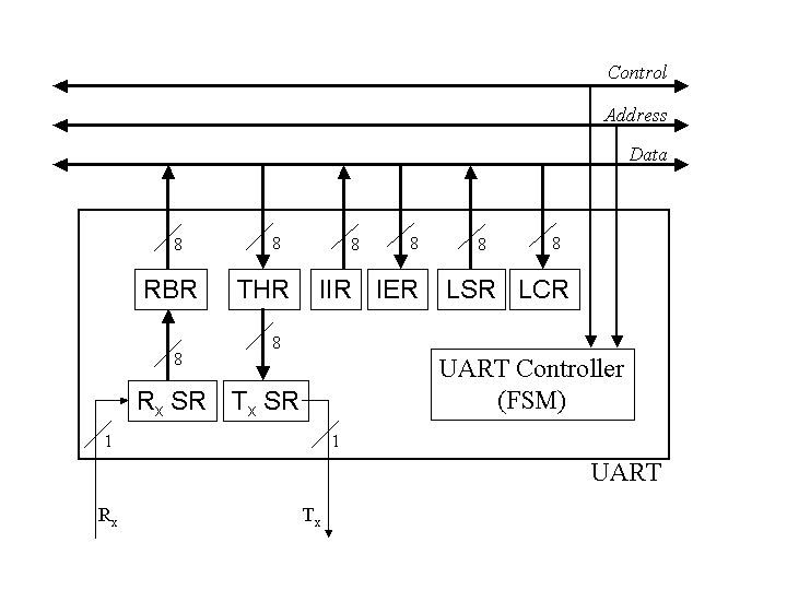
Internally, a UART has several different registers that the CPU can
read and write. The following table lists just a few of them. The
left column lists the addresses the CPU uses to access these registers
for a UART being used for COM1 in a standard PC.
| Address
| Name
| Function
|
| 0x3F8
| RBR
| Read Buffer Register. The CPU reads data bytes from this
register.
|
| 0x3F8
| THR
| Transmitter Holding Register. The CPU writes data bytes to this
register.
|
| 0x3F9
| IER
| Interrupt Enable Register. The CPU writes a byte to this
register to tell the UART when to generate interrupts. Individual
bits within the byte indicate whether to generate an interrupt when
the RBR is full, when the THR is empty, or when an error condition
is detected.
|
| 0x3FA
| IIR
| Interrupt Identification Register. The CPU reads this register
to find out why the UART generated an interrupt.
|
| 0x3FB
| LCR
| Line Configuration Register. The CPU writes bytes to this
register to configure parameters like baud rate (the speed at which
bits are sent and received) and parity (error checking) options.
|
| 0x3FD
| LSR
| Line Status Register. The CPU reads from this register to
find out whether the RBR is full, whether the THR is empty, or
whether an error condition has been detected.
|
This table is far from complete, but it is accurate as far as it
goes. The registers described here give us enough to work with so we
can see how a Device Controller works.
To understand how a UART operates we also need to introduce two
additional registers that are not in the table, and which the CPU
cannot access directly. These are the shift registers connected to
the Rx and Tx wires. The Rx shift
register (Rx SR) is an 8 bit register that receives
incoming serial data. When 8 data bits have arrived, the
Rx SR is transferred in parallel into the 8-bit RBR.
While waiting for the CPU to read from the RBR, the Rx SR
can start receiving bits from the next input byte on the
Rx line. Likewise, there is a Tx shift
register (Tx SR) that gets loaded from the THR in
parallel, and then shifts the bits out over the Tx wire
one at a time. While the Tx SR is transmitting a byte,
the CPU can write another data byte to the THR.
Software Layers
The descriptions of the registers in the table above used phrases
like, "the CPU reads ..." and "the CPU writes ...". Statements like
this means that some software, called a Device Driver, executes
the CPU's in and out ISA-level instructions. For
example, the Intel Architecture instruction inb 0x3F8 would
read a byte from the RBR of the COM1 UART into the CPU's "AL"
register.
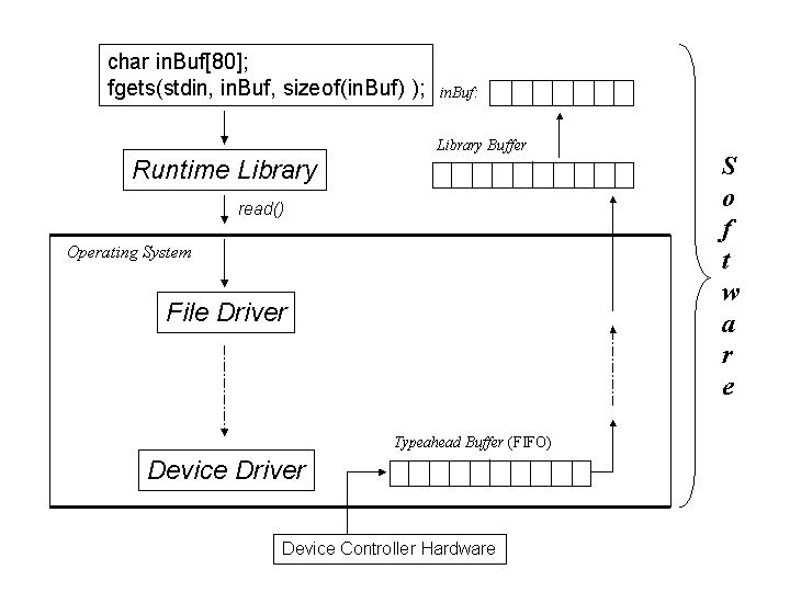
Each Device Controller attached to the I/O Bus has its own Device
Driver in the operating system. As the figure below indicates, the
Device Driver is the lowest of several layers of software involved in
I/O operations. At the top of the figure, a program (this could be a
C or C++ program) has set up an array of bytes named inBuf and
calls a function to read a string of characters into the array. We'll
assume that the string the program reads consists of characters a user
types on a keyboard that is connected to the Rx input line
of a UART.
The fgets() function is part of the C or C++ Runtime
Library that gets linked to all C/C++ programs. The library
functions manage their own buffer of data. If there are enough data
bytes available in the library buffer, the call to fgets() is
just a quick function call that copies the requested string from the
library buffer to inBuf, and the user's program spends
virtually no time at all making the function call. But if there are
not enough bytes in the library buffer to satisfy the call to
fgets(), it calls read(), which is an Operating System
Call that goes through several layers of software in the OS until
finally some code extracts bytes from the Device Driver's "typeahead
buffer" shown in the lower part of the figure. When the device
driver reads a byte from the RBR, it puts it into the tail of the
typeahead buffer FIFO (first-in, first-out queue). This buffer is
called a "typeahead" buffer because the user can type characters
before any program tries to read them, and they will be kept here
until a read() system call consumes them and passes them back
up to the library's buffer. But if the typeahead buffer doesn't have
a complete string in it when the read() function is executed,
the program will be blocked until the user types enough characters
for the Device Driver to put into the typeahead buffer for the
read() function to complete.
The boundary between the Runtime Library and the Operating System
is an important one. The input and output instructions that Device
Drivers execute are "privileged" instructions that will cause the CPU
to generate a fault (a hardware-generated exception) if code in the
library tries to execute them. Switching the CPU from non-privileged to
privileged mode is a very time-consuming operation compared to a
simple function call, a topic (hopefully) covered in your Operating
Systems course. The Runtime Library is designed to minimize the
number of system calls a program has to make as much as possible.
Device Driver Designs
Polled ("Programmed") I/O
Before reading from the RBR, the device driver must read from the
LSR to determine if there is a new byte available there yet or not. A
simple way to program a device driver it to code an endless loop that
looks something like this:
        char  lsr;
        char  rbr;
        char  typeahead[100];
        int   nextPut = 0;
        for ( ;; )
        {
          lsr = inbyte( 0x3FD );
          if ( (lsr & 0x01) != 0 )
          {
            rbr = inbyte( 0x3F8 );
            typehead[ nextPut++ ] = rbr;
          }
        }
There are several things to say about the above code. The first
is that it is written in C/C++, where the size of a char is
one byte. (In Java, a char is two bytes.) The second is that it
assumes there is a function or macro named inbyte() that takes
an I/O address as an argument, and returns a byte that it reads from
that address. The third is that the sample code assumes that the bit
in the rightmost position of the LSR (0x01) gets turned on by the
UART's control logic every time the Rx SR fills up and is
transferred to the RBR, and that this bit gets turned off when the
CPU reads from the RBR. Fourth, the typeahead array needs to be
implemented as a "bounded buffer," which means that all the code for
making nextPut wrap around to the beginning and all the logic
for producer-consumer synchronization would need to be added in a
real Device Driver. Again, that's a topic for your Operating Systems
course to cover.
The endless loop in this code is called a "polling loop." The
device driver asks the device controller ("polls the device
controller") by reading the LSR to find out if there is a new data
byte to read, and reads the byte if there is. Whether there is
anything to read or not, the code then just goes back and polls the
LSR again immediately. This coding technique dedicates all the CPU's
fetch-execute cycles to polling and reading the Device Controller,
which leaves no time for the CPU to execute anything else.
(Including the consumer side of the producer-consumer relationship!)
A modified version of this polling technique might actually be
appropriate in a situation where a simple CPU is dedicated to
processing data from a high-speed source such as a laboratory
instrument. But in general, it is too restrictive for general
purpose computing.
Interrupt-Driven I/O
Instead of constantly polling the Device Controller, the Device
Driver can configure the Device Controller to send a special signal
to the CPU whenever the LSR changes in an "interesting." way.
(Interesting means, for example, when a new byte is loaded into the
RBR from the Rx SR but not when the CPU reads from the
RBR, even though both events cause the LSR to change.) This signal
is called an Interrupt ReQuest (IRQ). An Intel
processor has just one IRQ wire going into it, which can be thought
of as a separate wire among the control wires of the I/O bus. (A
separate device called a Programmable Interrupt Controller handles
the management of different IRQs coming from the various Device
Controllers in the system.)
Instead of dedicating all the CPU's execution cycles to polling
Device Controllers, the operating system can scheule other programs to
run while a program is waiting for I/O. The CPU fetch-execute cycle
we looked at in Chapter 6 is modified so that the CPU checks the
status of the IRQ line just before each instruction fetch. If it is
true, the CPU writes the contents of all the registers, including the
psr (which contains the condition code bits) into a reserved
area of memory, and fetches the next instruction from the code in the
device driver that reads the LSR, which by definition will indicate
either that the RBR is ready for reading, the THR is ready for
writing, or that an error has occurred that requires some sort of
recovery action. This part of the Device Driver that gets called by
the CPU itself in response to an IRQ is called an interrupt
handler or an interrupt service routine (ISR). When the
ISR finishes polling and reading or writing the Device Controller
registers, it executes a "return from interrupt" instruction, which
signals the CPU that it can resume the interrupted program by
loading all the registers from the reserved area of memory and
fetching the instruction addressed by the pc register.
Managing interrupts from multiple Device Controllers and scheduling
multiple programs to use the CPU in the intervals between interrupts
are, yet again, topics for your Operating Systems course.
Direct Memory Access
If you look at the polling loop code above and think about what is
happening, you can see that each byte of data gets read into the CPU
and then written out from the CPU to memory, requiring two bus cycles
each. (Because the program uses the lbr variable in memory
there are actually two overhead bus cycle that could be eliminated by
writing:
typeahead[ nextPut ] = inByte( 0x3F8 );
A good compiler would optimize the first version of the code to
eliminate the extra cycles.)
For a low-speed controller like a UART, the overhead of moving data
from the Device Controller to the CPU and from the CPU to memory is
not worth worrying about. But devices like disk drives can place an
unnecessarily heavy load on the system if every byte being read from
the drive has to cause an I/O interrupt and two bus cycles to get into
a memory buffer. The solution is to design the disk drive's device
controller so it can be operated in Direct Memory Access (DMA)
mode.
A DMA-capable device controller has registers to which the CPU can
write the address of the beginning of a buffer in memory and it's
size. After writing the address and size values into these
registers, the CPU writes a value to another register in the controller
that tells it to start a DMA transfer. The controller then writes
the data directly into the memory buffer as it arrives from the disk
drive, and only sends one IRQ to the CPU when the entire transfer has
completed. The efficiency gained is the elimination of half the bus
cycles due to transferring the bytes to the CPU, and the elimination
of almost all the interrupt processing. The bus, however must be
designed to arbitrate between the CPU and the device controller,
since both will be trying to use the bus at the same time. The CPU
can be fetching instructions from one part of memory while the disk
controller is trying to write data to another part of memory using
the same bus, but only one bus transfer can actually occur at a
time.
As with all the rest of the material in this web page, extending
this description of DMA transfers to writing as well as to reading
functions is left as an exercise for the student.(!)